HMC283LM1
v04.1201
Typical Applications
The HMC283LM1 is ideal for:
• Millimeterwave Point-to-Point Radios
• LMDS
• SATCOM
11
LINEAR & POWER AMPLIFIERS - SMT
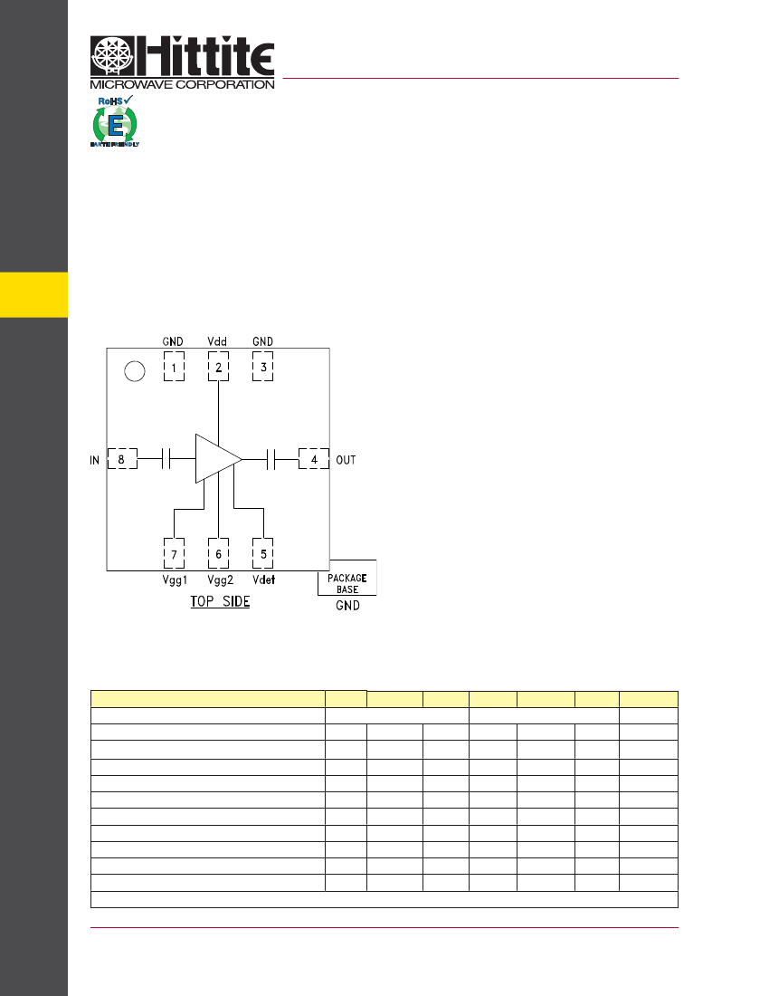
Functional Diagram
D
E
U
IN
T
N
O
T
C
C
S
U
I
D
D
O
R
P
Features
SMT mmWave Package
Psat Output Power: +21 dBm
High Gain: 21 dB
No External Matching Required
SMT MEDIUM POWER GaAs MMIC
AMPLIFIER, 17 - 40 GHz
o
ed f
The
a Medium
end
a HMC283LM1 ischip carrierPower Amplifier (MPA)
package covering 17
m
in SMT leadless
om
to 40 GHz. The LM1 is a true surface mount broadband
Rec
millimeterwave package offering low loss & excel-
Not
lent I/O match preserving MMIC chip performance.
Utilizing a GaAs PHEMT process, the device offers
20 dB gain and +21 dBm output power from a bias
supply of +3.5V @ 300mA. As an alternative to chip-
and-wire hybrid assemblies the HMC283LM1 elimi-
nates the need for wirebonding, thereby providing
a consistent connection interface for the customer.
The amplifier may be used as a frequency doubler.
A built-in-test pad (Vdet) allows monitoring of micro-
wave output power. All data is with the non-hermetic,
epoxy sealed LM1 packaged MPA device mounted in
a 50 ohm test fixture.
General Description
r Ne
w
s
ign
Des
Electrical Specifi cations,
T
A
= +25° C, Vdd= +3.5V*, ldd = 300 mA
Parameter
Frequency Range
Gain
Gain Variation over Temperature
Input Return Loss
Output Return Loss
Reverse Isolation
Output Power for 1 dB Compression (P1dB)
Saturated Output Power (Psat)
Output Third Order Intercept (IP3)
Noise Figure
Supply Current (Idd)
6
4
30
14
17
22
15
Min.
Typ.
17 - 40
20
0.05
10
7
40
18
21
27
10
300
330
0.07
6
4
35
14
17
21
17
Max.
Min.
Typ.
21 - 30
22
0.05
12
8
45
18
21
27
10
300
330
0.07
Max.
Units
GHz
dB
dB/°C
dB
dB
dB
dBm
dBm
dBm
dB
mA
*Vdd = +3.5V, adjust Vgg = Vgg1, Vgg2 between -2.0 to +0.4V to achieve Idd = 300 mA typical.
11 - 2
For price, delivery, and to place orders, please contact Hittite Microwave Corporation:
20 Alpha Road, Chelmsford, MA 01824 Phone: 978-250-3343 Fax: 978-250-3373
Order On-line at www.hittite.com


