1. 费米架构

FERMI架构图
SM
- SM Streaming multi-processors with multiple processing cores
- Each SM contains 32 processing cores
- Executive in a Single Instruction Multiple Thread ( SIMT ) fashion
- Up to 16 SM on a card for a maximum of 512 compute cores
- Instruction Cache ?K 缓存指令
- Warp Scheduler Warp 调度器
- Dispatch Unit 将指令发送的要执行的warp中
- Register File 寄存器文件
- core 也叫 streaming processor,相当于CPU的ALU单元
- LD/ST load 和 store 单元,负责访存
- SFU special function unit 特殊函数单元 cos sin
- L1 cache /shared mem 64K可配置
计算能力 2.x Fermi 关于cache 的描述
const cache
A multiprocessor also has a read-only constant cache that is shared by all functional units and speeds up reads
from the constant memory space, which resides in device memory.
data cache
There is an L1 cache for each multiprocessor and an L2 cache shared by all multiprocessors,
both of which are used to cache accesses to local or global memory, including temporary register spills.
The cache behavior (e.g., whether reads are cached in both L1 and L2 or in L2 only) can be partially configured on
a per-access basis using modifiers to the load or store instructionThe same on-chip memory is used for both L1 and shared memory: It can be configured as 48 KB of shared memory and 16 KB of L1 cacheor as 16 KB of shared memory and 48 KB of L1 cache, using cudaFuncSetCacheConfig()/cuFuncSetCacheConfig():
b) 开普勒架构
c) Maxwell
d) 最新的Pascal架构
e) 讲一下 sp sm sfu ld/st
f) Regeister file
g) Shared memory l1cache
h) l2cache
2. GPU计算流程
a) 取指令
b) 译码
c) 执行
d) 写回
e) Warp调度的特点
f) 内存请求合并的特点
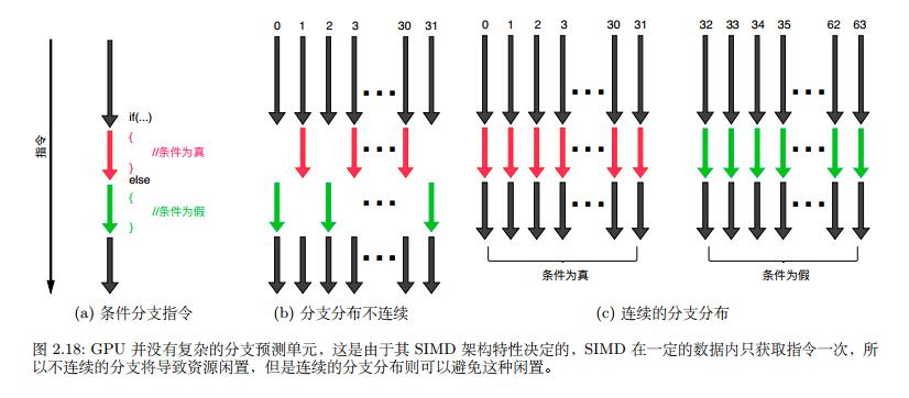
g) Warp分歧的处理
3. 存储分层介绍 各层主要的特点,以及发现的问题
a) 片上存储
i. Register file
ii. Shared memory
iii. L1Dcache
iv. Bypass
b) 片外存储
i. L2cache
ii. DRAM 调度


