目录
1. Conductivity and two general modes of charge transport in solid-state materials (Fig. 1b)
2. What is Bravais lattice, what is basis and what is crystal lattice (Fig. 2). The differences between five possible Bravais lattices in two dimensions (Fig. 2.3)
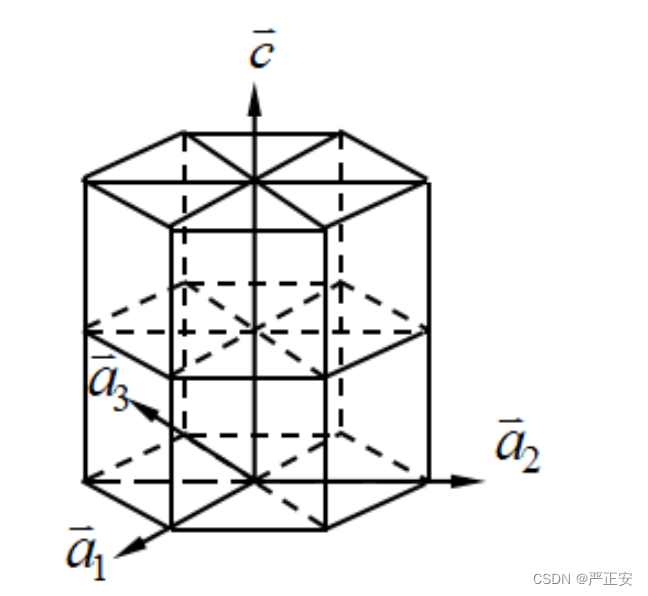
3. What are the Miller indexes (hkl). Also, describe Miller indexes (hkil) for hexagonal structures
3. Being able to draw atomic structure of graphite, graphene and diamond.
4. Examples of isotropic and anisotropic properties
5. 2D lattices in real and in reciprocal space. Being able to draw Wigner-Seitz primitive unit cell (real space) and the first Brillouin zone (reciprocal space), see for example Fig. 2.8 in the book
6.Basic principle of LEED and what knowledge can you obtain from a LEED measurement (Fig. 2.10)
7.Basic principle of STM and what knowledge can you obtain from a STM measurement (Fig. 2.14 and Fig. 2.20) 8. Basic principle of STS and what knowledge can you obtain from a STS measurement (e.g. Fig. 2.16, Fig. 2.18, Fig.2.19)
8.Basic principle of AFM and what knowledge can you obtain from a AFM measurement (Fig. 2.21)
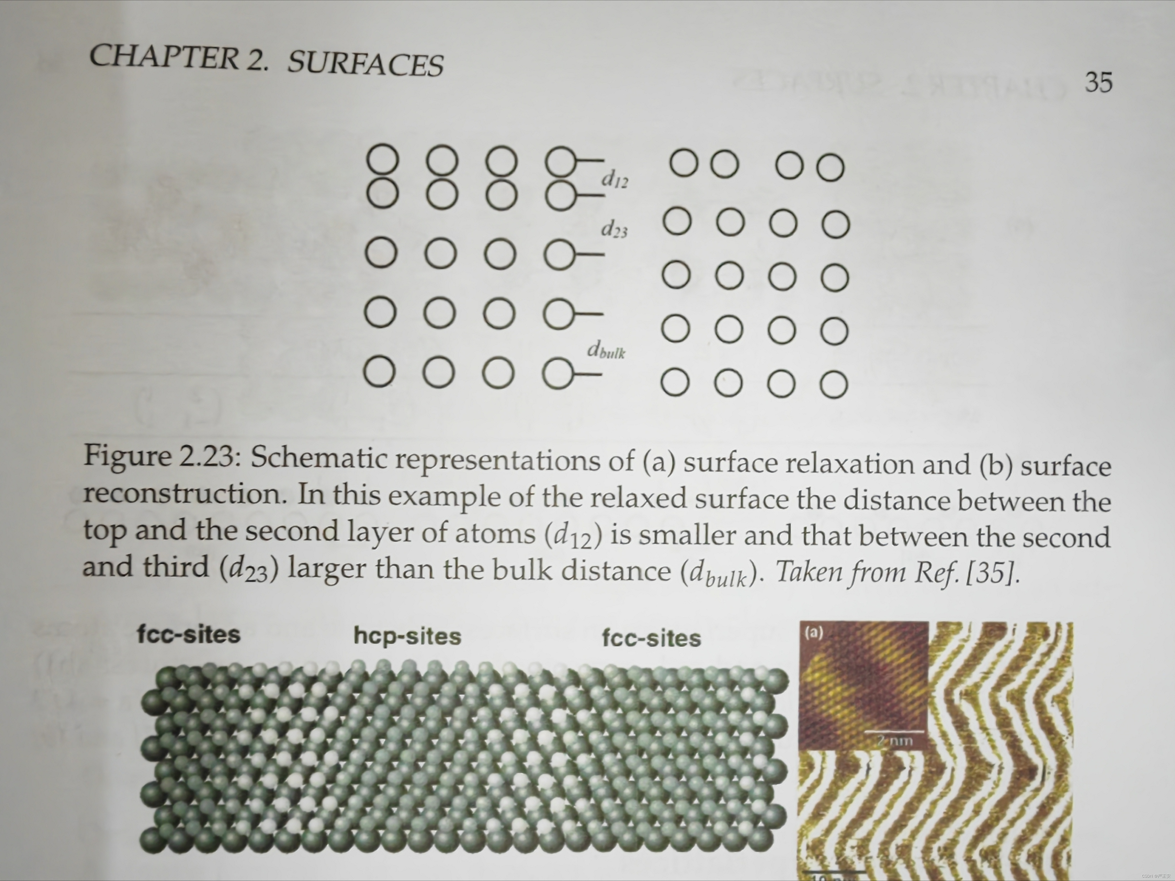
9.Difference between surface relaxation and surface reconstruction (page 34, and also Fig. 2.23, Fig. 2.24)
10. Surface superlattice and being able to determine matrix notation (Fig. 2.25)
11. What are commensurate and incommensurate. When incommensurate lattice is formed? (page 36, and also Fig.2.25b)
12. Domains, grains, domain walls, and grain boundaries (being able to explain what is what)
13. Examples of defects in bulk crystals structures and in surface (e.g. Fig. 2.28)
14. I-V plots for resistors (ohmic contact) and for diodes (Fig. 3.1), also draw p-n junction energy band diagram to explain non-linear I-V characteristic of p-n junction diodes
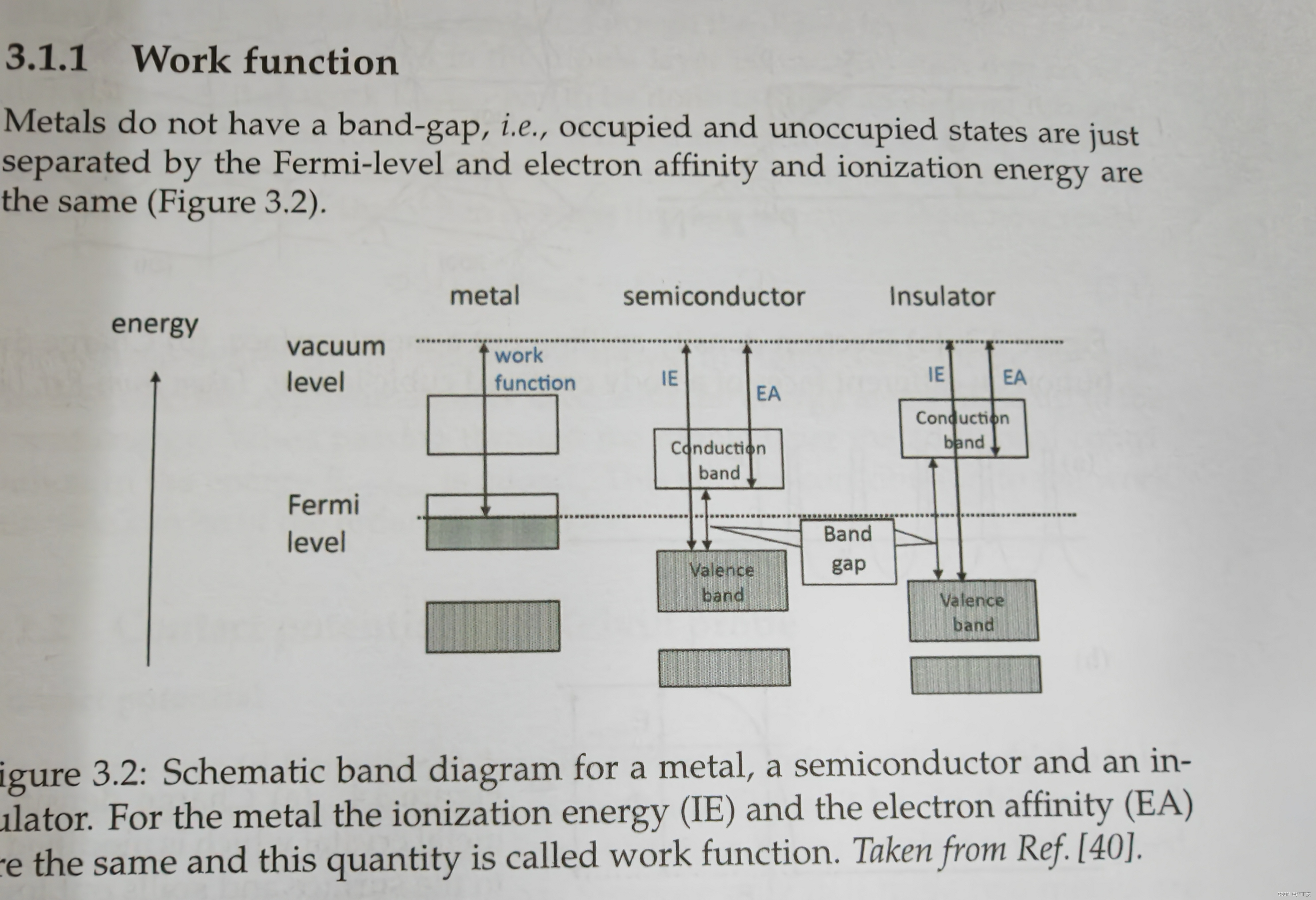
15. Draw band diagram for metals, semiconductors and insulators (e.g. Fig. 3.2), and explain the difference between three classes of materials
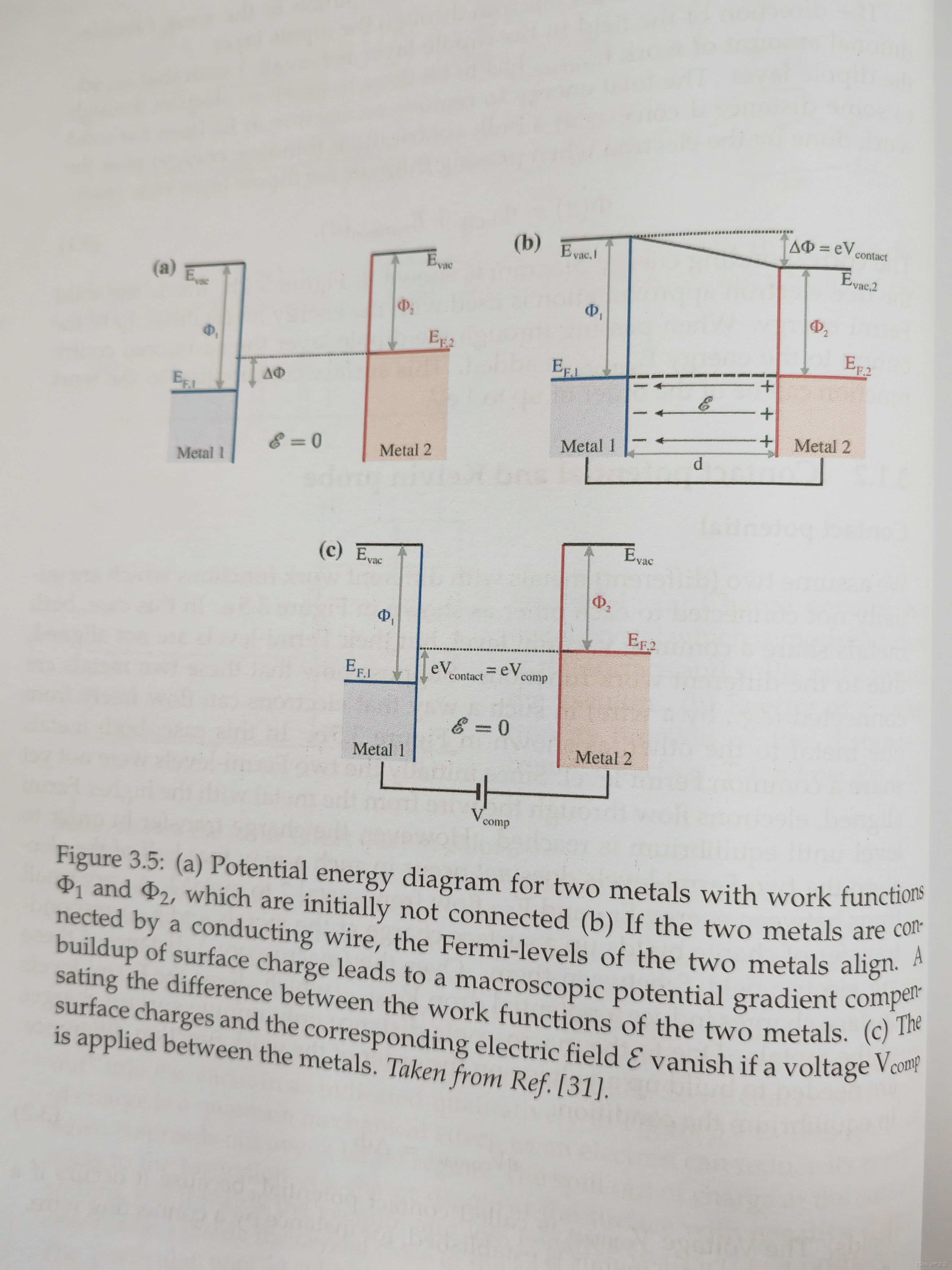
16. Contact potential between two metal contact. Being able to draw and describe band diagrams a) before the contact, b) after the contact, c) after the compensating voltage was applied to the contact (Fig. 3.5) 18. Schottky contact as diode (Fig. 3.12)
17. Surface photovoltage (Fig. 3.15)
18. Thin film growth: three growth modes (Fig. 4.3a)
19. Thin film growth: examples of growth processes (Fig. 4.3b)
20. Microstructure: difference between single crystals, fiber-textured thin films and 3D polycrystalline thin films (Fig.4.5)
21. Simplified mixing scenarios for molecular crystals and being able to explain the factor that determines whether there will be phase separation, OR formation of a co-crystal, OR random mixture (Fig. 4.6)
22. Basic principle of X-ray diffraction and what knowledge can you obtain from an X-ray diffraction measurement(Fig. 4.11)
23. Physisorption vs. Chemisorption (page 84, also Fig. 4.19)
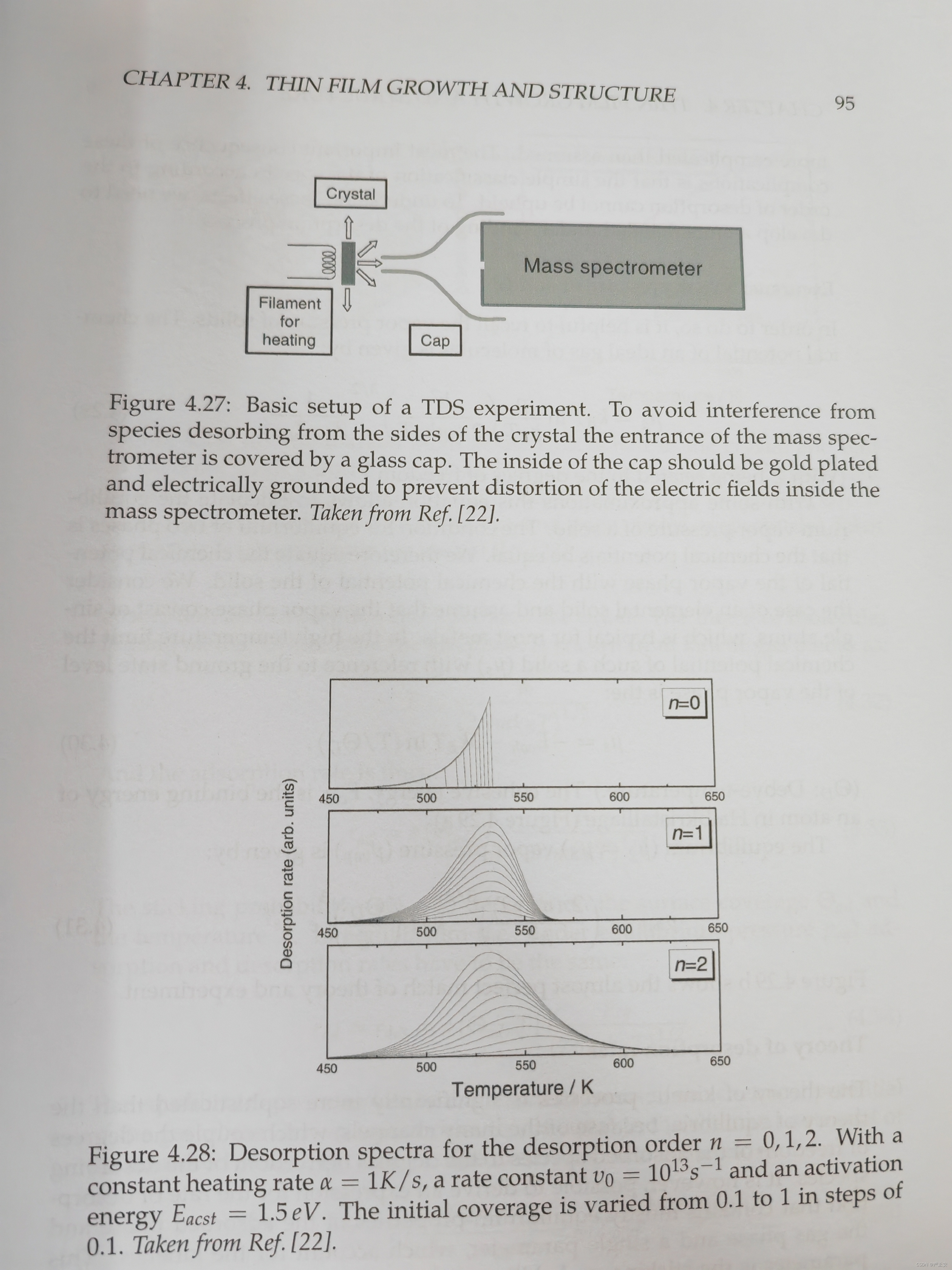
24. Basic principle of TDS and what knowledge can you obtain from a TDS measurement (Fig. 4.27, Fig. 4.28, Fig.4.30)
25. Excitons. Being able to describe the difference between Wannier-Mott excitons and Frenkel excitons (chapter.1.4 and Fig. 5.8a)
1. Conductivity and two general modes of charge transport in solid-state materials (Fig. 1b)
coherent band transport(相干带运输)and hopping transport(跳跃运输)
2. What is Bravais lattice, what is basis and what is crystal lattice (Fig. 2). The differences between five possible Bravais lattices in two dimensions (Fig. 2.3)
A crystal structure is defined by the so-called bravais lattice and so-called basis.
描述任何晶体固体的一个基本概念是Bravais点阵(晶格),它规定了晶体重复单元排列的周期阵列。这些单位本身可能是单个原子、原子群、分子、离子等,但布拉维晶格仅概括了基本周期结构的几何结构,而不管实际单位可能是什么。以下是两种等效的定义:

3. What are the Miller indexes (hkl). Also, describe Miller indexes (hkil) for hexagonal structures
晶向:表示晶体中点阵方向的指数,由晶向上阵点的坐标值决定。
晶面:表示晶体中点阵平面的指数,由晶面与三个坐标轴的截距值决定。
晶向族:晶体中原子排列情况相同但空间位向不同的一组晶向称为晶向族。
晶面族:晶体中具有等同条件,即原子排列情况和晶面间距完全相同,只是空间位向不同的各组晶面称为晶面族。
晶带轴:所有平行或相交于某一晶向直线的晶面构成一个晶带,此直线称为晶带轴。属此晶带的晶面称为共带面。
3. Being able to draw atomic structure of graphite, graphene and diamond.
4. Examples of isotropic and anisotropic properties
5. 2D lattices in real and in reciprocal space. Being able to draw Wigner-Seitz primitive unit cell (real space) and the first Brillouin zone (reciprocal space), see for example Fig. 2.8 in the book

6.Basic principle of LEED and what knowledge can you obtain from a LEED measurement (Fig. 2.10)
7.Basic principle of STM and what knowledge can you obtain from a STM measurement (Fig. 2.14 and Fig. 2.20) 8. Basic principle of STS and what knowledge can you obtain from a STS measurement (e.g. Fig. 2.16, Fig. 2.18, Fig.2.19)
8.Basic principle of AFM and what knowledge can you obtain from a AFM measurement (Fig. 2.21)
9.Difference between surface relaxation and surface reconstruction (page 34, and also Fig. 2.23, Fig. 2.24)
10. Surface superlattice and being able to determine matrix notation (Fig. 2.25)
11. What are commensurate and incommensurate. When incommensurate lattice is formed? (page 36, and also Fig.2.25b)
12. Domains, grains, domain walls, and grain boundaries (being able to explain what is what)
13. Examples of defects in bulk crystals structures and in surface (e.g. Fig. 2.28)
14. I-V plots for resistors (ohmic contact) and for diodes (Fig. 3.1), also draw p-n junction energy band diagram to explain non-linear I-V characteristic of p-n junction diodes
15. Draw band diagram for metals, semiconductors and insulators (e.g. Fig. 3.2), and explain the difference between three classes of materials
16. Contact potential between two metal contact. Being able to draw and describe band diagrams a) before the contact, b) after the contact, c) after the compensating voltage was applied to the contact (Fig. 3.5) 18. Schottky contact as diode (Fig. 3.12)
17. Surface photovoltage (Fig. 3.15)

18. Thin film growth: three growth modes (Fig. 4.3a)
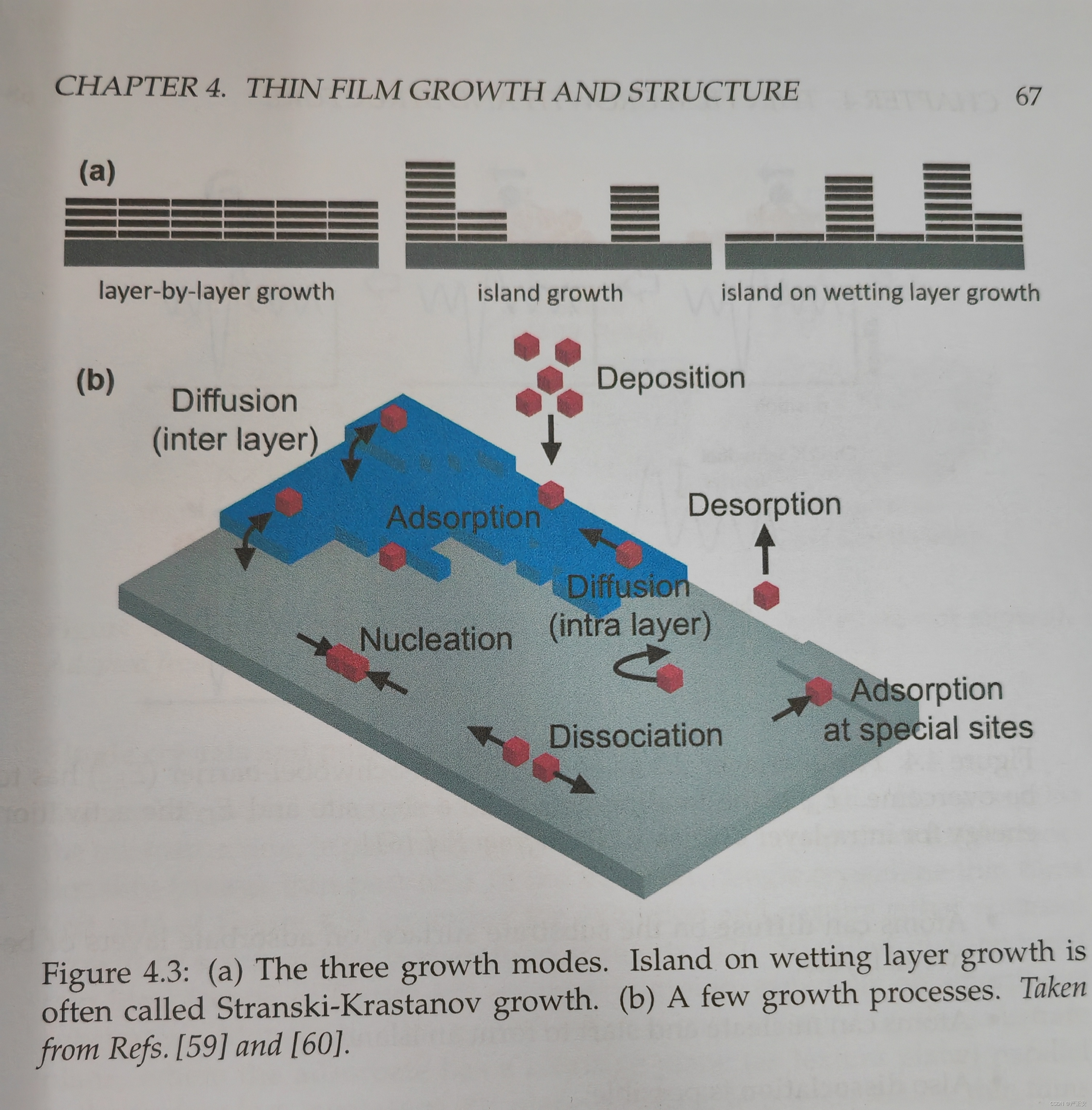
19. Thin film growth: examples of growth processes (Fig. 4.3b)

20. Microstructure: difference between single crystals, fiber-textured thin films and 3D polycrystalline thin films (Fig.4.5)

21. Simplified mixing scenarios for molecular crystals and being able to explain the factor that determines whether there will be phase separation, OR formation of a co-crystal, OR random mixture (Fig. 4.6)
22. Basic principle of X-ray diffraction and what knowledge can you obtain from an X-ray diffraction measurement(Fig. 4.11)

23. Physisorption vs. Chemisorption (page 84, also Fig. 4.19)