文章目录
- drain currunt
- Threshold Voltage (VTH)
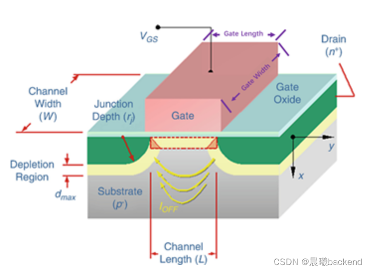
- channel length
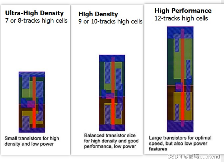
- track(Classification according to the Density)
- Standard Cell Layout
drain currunt

Drain current (Id) = uCox(W/L)[(Vgs-Vth)Vds-(1/2)Vds^2]
Cox=epision/tox#饱和电流计算公式:
#saturation current
**Id=(1/2) µ*Cox(W/L) *(Vgs-Vth)2**
- µ:为载流子的迁移速率 (老工艺时在温度和delay关系中占主导、温度越高,载流子的迁移速率降低,ld减小,delay变大)
- 单位面积氧化层电容,与tox成反比(tox越大,ld越小,cell delay越大)
- W/L:channel 宽长比
- Vgs-Vth:为过驱动电压 (先进工艺时在温度和delay关系中占主导、导致Temperature Inversion)
Threshold Voltage (VTH)
-
Threshold Voltage越大,cell delay越大,leakage power越小
-
LVT、RVT/SVT、HVT
- Low VT (LVT) - Fast because of low Gate Delay, but high leakage
- Standard VT (SVT) or Regular VT (RVT)
- High VT (HVT) - Low leakage, but slow because of high Gate Delay
-
HVT Cells are used in Non-critical paths to reduce Leakage Power while LVT Cells are used in Critical paths to met Timing
channel length
- 相同size的cell,channel length越小,channel W/L 越大, drain currunt越大,cell delay越小
- 沟道长度越短(注意gate length和
channel length(gate length-2*diffusion)区别),管子速度就越快,leakage也越大
track(Classification according to the Density)
- Track can be defined as a line on which metal layers are drawn. A track means one M1 Pitch. Height of Standard cell is generally measured in term of no. of tracks inside it. An example of 13T standard cell is given below in figure-5.

In the above example, the height of one track is 190 nm. So total height of cell is 13T = 2470 nm (13 x 190) and width is 5T = 950 nm (5 x 190).
- track 是PR中的布线轨道,用track之间的间距pitch来表征不同高度的stdcell (tracks mean routing resources),13 track stdcell 的高度是13*track_pitch ,(size越大、速度越快、功耗越高)
- Ultra High Density (UHD) - 7 Track or 8 Track
- High Density (HD) - 9 Track
- High Performance (HP) - 12 Track

-
Small transistor cells (6T Cells)
- Minimum area and low power
- Mobile applications
- Ultra-low-power applications
- Embedded microcontroller
-
Medium transistors cells (9T Cells)
- Balance area and performance
- General Computing
- GPU
- General-purpose circuit
-
Large transistors cells (12T Cells)
- Large area
- High performance and speed
- High-speed computing
- Critical blocks

Standard Cell Layout
At the top of the standard cell, there is VDD rail and bottom there is a VSS rail. Both the Power rails are drawn in the Metal-1 layer. In between the VDD rail and VSS rail there are three main regions, a nwell region, a gap of nwell and pwell and pwell region. nwell region is near to the VDD rail and pwell region is near the VSS rail. pMOS transistors are build inside the nwell, so all the pMOS transistors are in the top half of the cell and similarly, all nMOS are in the bottom half of the standard cell.

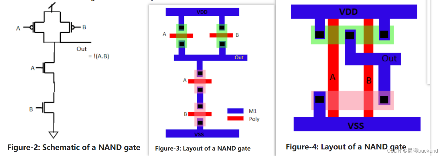
Layout of a schematic can be drawn in various ways. For example layout of a NAND gate can be drawn in following two different styles.

Figure-2 is showing the schematic of a NAND gate and figure-3 and figure-4 showing two different layouts of the schematic shown in the figure. In figure 3 both the nMOS are in not the same level, they are stacked but in the layout of figure 4 all nMOS are in one level and all pMOS are at one level. And in figure-3 gates are drawn horizontal and not common in nMOS and pMOS. But in figure-4, all the poly gates are drawn vertical and common to nMOS and pMOS both.
- There are many reasons PR preferring a layout style like in figure-4. Some of them are:
-
- Save Design Area: Both the nwell and pwell are in the same level for all the standard cell, so they can easily abut and make a common well which saves lots of areas.
-
- Easy placement for APR tool: All the standard cells have the same height and easily can be fit into the standard cell row so make it easy for APR (Automatic Place and Route) to place them. They also have power rails in the same location for all the standard cells, so power rails can also be abutted easily.
-
- Easy to route: All the pins of standard cells are in the intersection of horizontal and vertical tracks, So it becomes easy to route them by the APR tool
-


