视频链接
PCIE转串口和并口电路设计01_哔哩哔哩_bilibili
PCIe转串口和并口电路设计
1、PCIe转串并口电路设计基本介绍
2、PCIe转串口和并口的方案(京东)
2.1、PCIe转串口
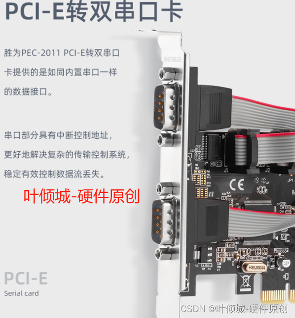
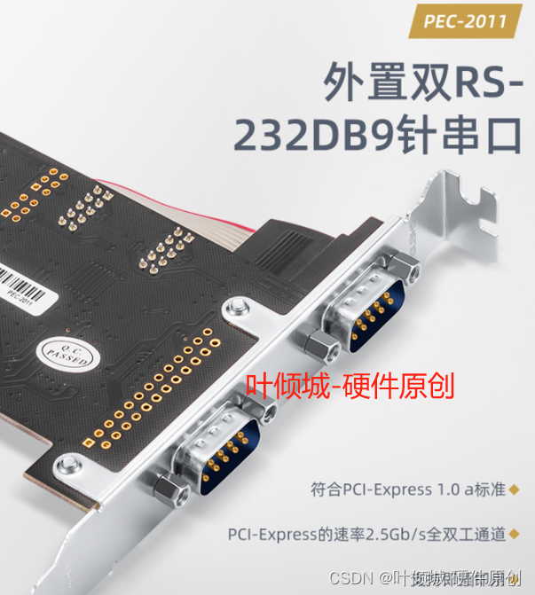
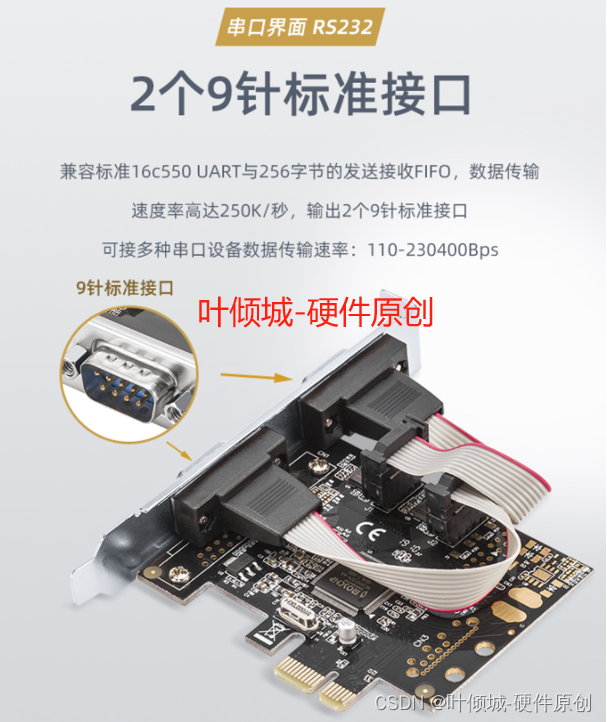
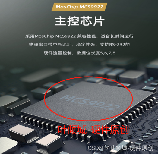
2.1.1、ASIX (亚信)MCS9922-PCIe转2路RS232扩展卡
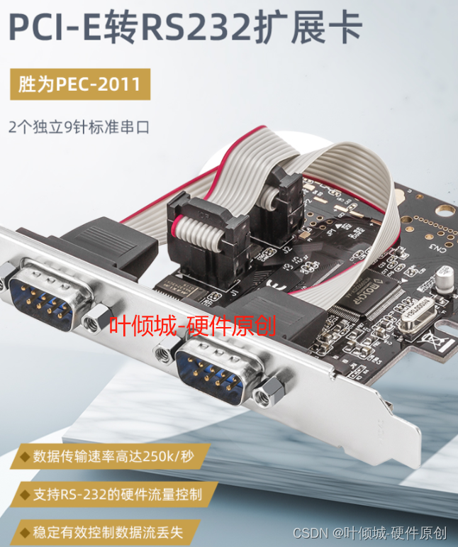
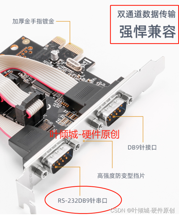
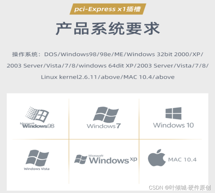
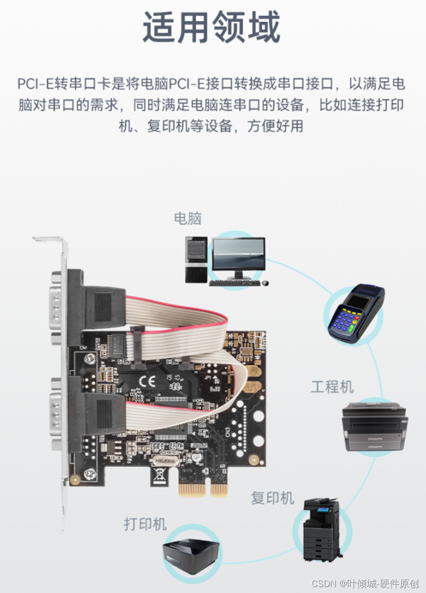
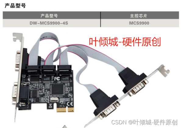
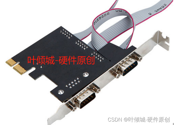
2.1.2、ASIX (亚信)MCS9900-PCIe转4路RS232扩展卡
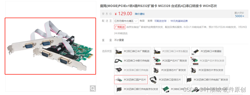
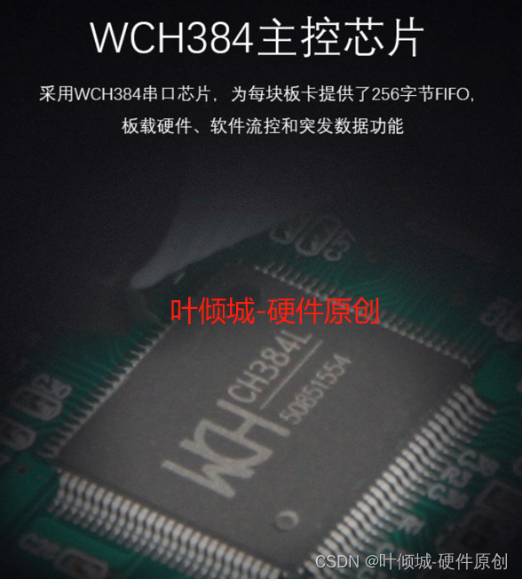
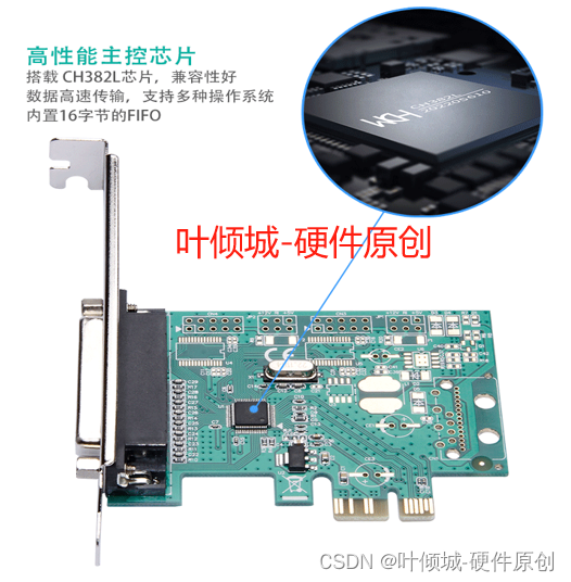
2.1.3、(国产)WCH-CH384L-pcie转串口工控4口扩展卡
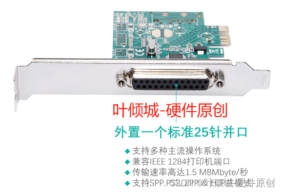
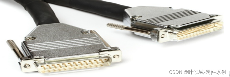
2.2、PCIe转并口
2.2.1、ASIX (亚信)MCS9901-PCIe转双串行和单并行控制器-I/O连接控制器

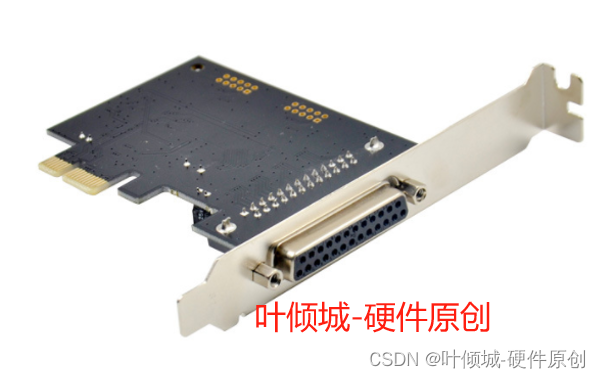
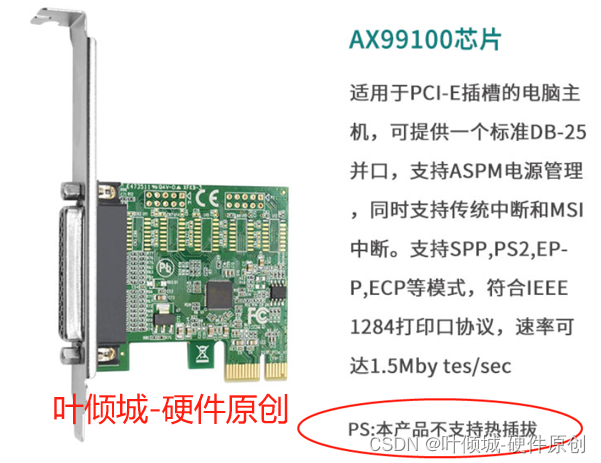
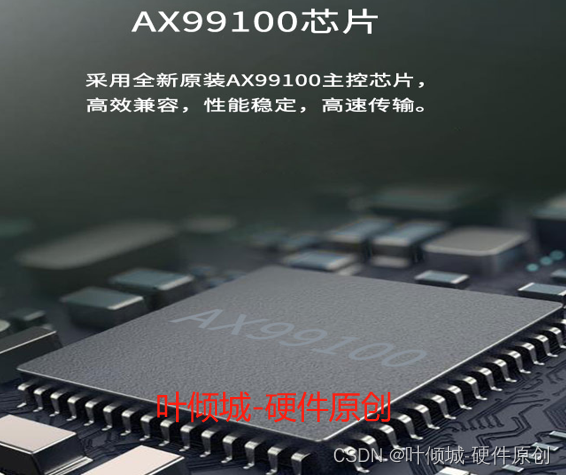
2.2.2、ASIX(亚信)MCS99100 PCIe转并口DB25打印机扩展卡

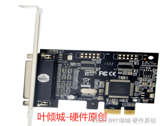
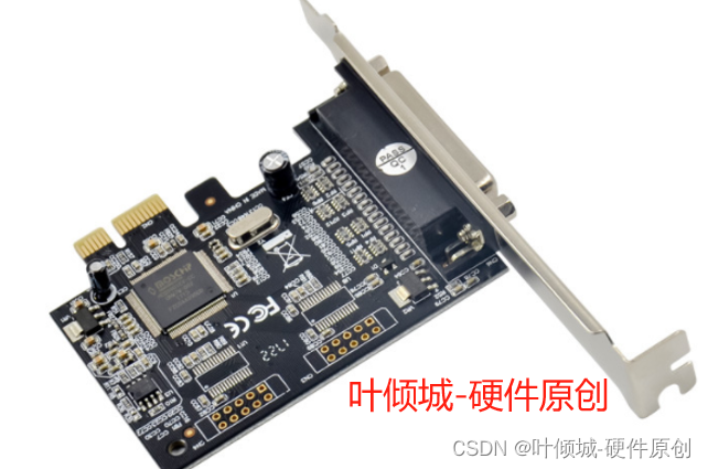
2.2.3、(国产)WCH CH382L PCIe转并口DB25转接卡
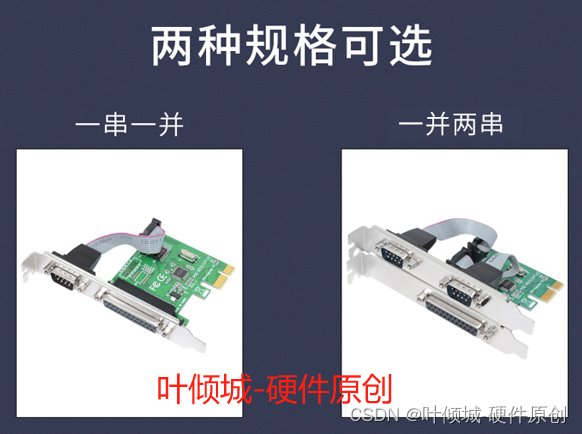
2.3、PCIe转串口和并口
3、串口和并口
3.1、串行接口(参考第4课)
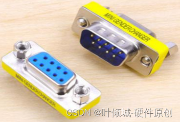
串口叫做串行接口,也称串行通信接口,即COM口。
DB9接口定义如下表,我们一般只用到其中的RXD、TXD、GND引脚,其他引脚在普通串口模式下一般不使用。
| PIN | 定义 |
| DCD | 数据载波检测 |
| RXD | 接受数据 |
| TXD | 发送数据 |
| DTR | 数据终端准备 |
| GND | 地线 |
| DSR | 数据准备就绪 |
| RTS | 请求发送 |
| CTS | 清除发送 |
| RI | 振铃提示 |
3.1、并行接口
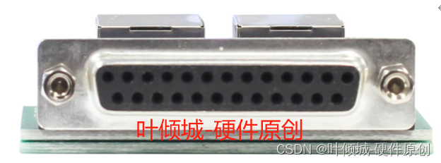
并口采用的是25针D形接头。所谓“并行”,是指8位数据同时通过并行线进行传送,这样数据传送速度大大提高,但并行传送的线路长度受到限制,因为长度增加,干扰就会增加,数据也就容易出错,目前,并行接口主要作为打印机端口等。
并口的工作模式:
1、SPP(Standard Parallel Port)
2、EPP(Enhanced Parallel Port)
3、ECP(ExtendedCapability Port)
母头连接器的管脚定义
管脚定义
| Pin nubmber | Pin Description |
| 1 | ----> #STROBE 数据选通 |
| 2 | D0 |
| 3 | D1 |
| 4 | D2 |
| 5 | D3 |
| 6 | D4 |
| 7 | D5 |
| 8 | D6 |
| 9 | D7 |
| 10 | <---- #ACK 应答脉冲 |
| 11 | <---- BUSY 忙 |
| 12 | <---- PE 打印纸尽 |
| 13 | <---- SLCT 选择 |
| 14 | ----> #AUTOFD 自动进纸 |
| 15 | <---- #ERROR 错误 |
| 16 | ----> #INIT 初始化 |
| 17 | ----> #SELIN 打印机选择输入 |
| 18 | GND |
| 19 | GND |
| 20 | GND |
| 21 | GND |
| 22 | GND |
| 23 | GND |
| 24 | GND |
| 25 | GND |
3.3、串口与并口的区别
4、套片、桥片、PCIE switch等基本介绍
4.1、套片(不需要)
4.2、PCIE switch

4.3、桥片
4.4、CPU本身自带的PCIE接口
5、以超威主板为例
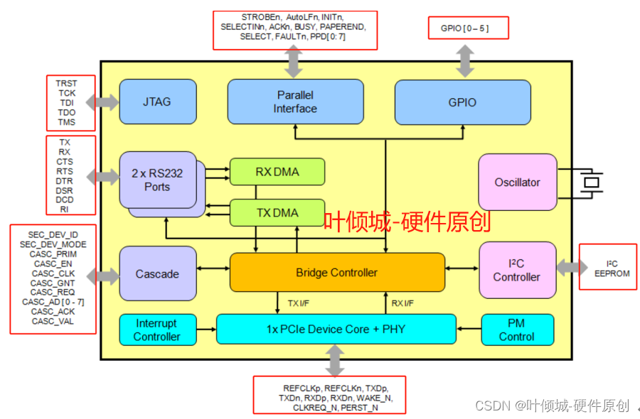
6、PCIe转串并口(以MCS9901为例)
MCS9901CV-CC是一种单通道多功能PCIe I/O控制器。支持2个串口,1个并口和6个GPIO口。
6.1、结构框图
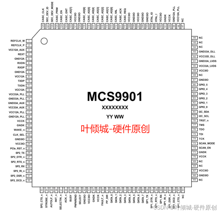
6.2.1、Power supply (★)
对于电源电压,系统要求
| Pin | I/O | 定义 |
| VCC12A_AUX VCC12A VCC12A_PLL | PWR | 1.2V Analog Power Supply |
| VCCK | PWR | 1.2V Digital Power Supply |
| VCC33A_PLL VCC33A_AUX VCC33A_LVDS | PWR | 3.3V Analog Power Supply |
| VCC3IO VCC33D_DLL | PWR | 3.3V Digital Power Supply |
| GND12A GND12A_PLL GND33A_PLL GND33A_AUX GND33A_LVDS GND33A_DLL | PWR | Analog Ground |
| GNDK GND3IO | PWR | Digital Ground |
6.2.2、PCIe Interface Signals (★)
| Pin | I/O | 定义 |
| REFCLK_M REFCLK_P | I | PCIe PHY differential PLL reference clock. Cascade Mode: Pull down using 10K Resistor. |
| REXT | O | Bandgap External Resistor (Connect this pin to ground through an external resistor of 6.2KΩ, ±1%) |
| RXDN RXDP | I | PCIe PHY differential positive serial data input. Cascade Mode: Pull down using 10K Resistor. |
| TXDP TXDN | O | PCIe PHY differential negative serial data output. Cascade Mode: Leave this pin as “No Connection”. |
| WAKE_n | O | This is an active low signal used to reactivate the PCI Express slot’s main power and reference clocks. Cascade Mode: Leave this pin as “No Connection”. |
| CLK_SEL | O | Used to enable/disable clock of PCI Express card. |
| PCIe_RST_n | I | Active low asynchronous reset from PCIe RC |
6.2.3、Serial Port Interface Signals (★)
Serial Port 1 & Serial Port 2
| Pin | I/O | Description |
| SP1_TX SP2_TX | O | Transmit data out to transceiver or IrDA data out to IR LED |
| SP1_DTR_n SP2_DTR_n | O | Data terminal ready (Active Low) |
| SP1_RTS_n SP2_RTS_n | O | Request to send (Active Low) |
| SP1_RX SP2_RX | I | Serial receives data in from transceiver or IrDA data in from IrDA detector. |
| SP1_RI_n SP2_RI_n | I | Ring Indicator (Active Low) |
| SP1_DSR_n SP2_DSR_n | I | Data Set Ready (Active Low) |
| SP1_DCD_n SP2_DCD_n | I | Data Carrier Detect (Active Low) |
| SP1_CTS_n SP2_CTS_n | I | Clear to send (Active Low) |
6.2.4、Parallel port Interface signals (★)
| Pin | I/O | Description |
| STROBE_n | O | Set active low by the host to transfer data into the input latch of the peripheral. Data are valid while STROBE_N is low. |
| AUTOLF_n | O | The interpretation of this signal varies from peripheral to peripheral. Set low by host to put some printers into auto-line feed mode |
| INIT_n | O | Pulsed low by the host in conjunction with IEEE 1284 Active low to reset the interface and force a return to Compatibility Mode idle phase |
| SELECTIN_n | I/O | Set low by host to select peripheral |
| ACK_n | I | Pulsed low by the peripheral to acknowledge transfer of a data byte from the host |
| BUSY | I | Driven high by the peripheral to indicate that it is not ready to receive data |
| PAPEREND | I | Driven high by the peripheral to indicate that is has encountered an error in its paper path. The meaning of this signal varies from peripheral to peripheral. Peripherals shall set FAULT_N low whenever PAPEREND is set high |
| SELECT | I | Set high to indicate that the peripheral is online |
| FAULT_n | I | Set low by the peripheral to indicate that an error has occurred. The meaning of this signal varies from peripheral to peripheral |
| PP_DIR | O | Set low to indicate a data transfer direction of peripheral to host and set high to indicate a data transfer direction of host to peripheral |
| DATA_[0:7] | I/O | Driven by the host in Compatibility Mode and the negotiation phase, not used in Nibble Mode, and bidirectional in all other modes |
6.2.5、Cascade Interface Signals
级联信号接口
| Pin | I/O | Description |
| CASC_REQ | I/O | To request the arbiter to grant access to CASC_AD bus |
| CASC_ACK | I/O | Asserted by slave, in response to CASC_VAL, when it is ready to accept transfer |
| CASC_VAL | I/O | 1:address/data/command on CASC_AD [7:0] is valid 0: CASC_AD is not valid |
| CASC_AD[0:7] | I/O | To transfer Address / Data and control words |
| CASC_GNT | I/O | Grant to access of CASC_AD bus |
| CASC_EN | I | 1 : cascade mode enabled 0 : cascade mode disabled |
| CASC_PRIM | I | Chip is cascade secondary. Leave this pin as “No Connection” |
| SEC_DEV_MODE | O | For Non-Cascade applications, leave this pin as No Connect. When MCS9901CV-CC is used as Cascade Secondary Device, connect this pin to corresponding pin of the Cascade Primary Device. |
| SEC_DEV_ID | I | Leave this pin as “No Connection” |
| CASC_CLK | O | Pull down using 1K resistor |
6.2.6、I2C Interface Signals (★)
| Pin | I/O | Description |
| I2C_SCL | I/O | 2-Wire EEPROM Clock |
| I2C_SDA | I/O | 2-Wire EEPROM Data in/out. |
6.2.7、GPIO Interface Signals
| Pin | I/O | Description |
| GPIO_[0:5] | I/O | General Purpose I/O signal |
6.2.8、Clock/Crystal Oscillator Interface Signals(★)
| Pin | I/O | Description |
| XTAL_I | I | Crystal input for PLL, 24~42MHz |
| XTAL_IO | I/O | Feedback signal for the oscillator pad |
6.2.9、Test Mode Signals (★)
| Pin | I/O | Description |
| SCAN_EN | I | Scan enable signal |
| SCAN_MODE | I | This signal is used as clock input in cascade mode. Cascade mode: Cascade Clock driven by ‘primary’ through ‘CASC_CLK’ should be interfaced to this pin. Non-Cascade Mode: Pull Down using 1K resistor. |
6.2.10、JTAG Interface Signals
| Pin number | I/O | Description |
| TCK | I | JTAG chain clock |
| TDI | I | JTAG chain input |
| TDO | O | JTAG chain output |
| TMS | I | JTAG chain Test mode select |
| TRST_n | I | JTAG Reset (pull-up is recommended on JTAG Reset) |
6.2.11、NC
集合:128pin LQFP
| Pin Description | 数目(个) |
| Power & Gnd | 41 |
| PCIe Interface Signals | 10 |
| Serial ATA Interface Signals | 8X2=16 |
| Parallel port Interface signals | 18 |
| Cascade Interface Signals | 17 |
| I2C Interface Signals | 2 |
| GPIO Interface Signals | 6 |
| Clock/Crystal Oscillator Interface Signals | 2 |
| Test Mode Signals | 2 |
| JTAG Interface Signals | 5 |
| NC | 9 |
合计: 41+10+16+18+17+2+6+2+2+5+9=128